Observation and Measurement of Probe Cards and Contact Probes
The spread of the fifth-generation mobile communications system (5G) and the products supporting it have further boosted the advancement of smaller and denser semiconductor devices. With this progress, the electrical inspection and analysis of various electronic components, such as integrated circuits (ICs) and large-scale integrated (LSI) circuits, require increasingly higher accuracy.
This section explains the basics of probe cards and contact probes, which are inspection instruments used for electrical inspection of semiconductor devices, and also introduces the latest examples of operations, such as observation and non-contact 3D measurement, using 4K images that help to maintain high levels of inspection accuracy.
- What Is a Probe Card?
- What Is a Contact Probe?
- Service Lives of Probe Cards and Contact Probes and Importance of Observation and Measurement
- The Latest Examples of Wear Observation and Dimension and Shape Measurement of Probe Cards and Contact Probes
- A 4K Digital Microscope That Improves the Efficiency of Various Operations Including Accuracy Maintenance of Electrical Inspection
What Is a Probe Card?
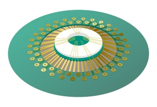
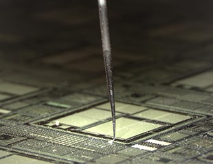
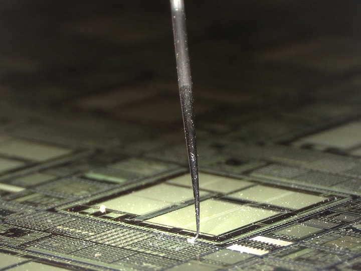
A probe card is an inspection instrument used in the inspection process of silicon wafers during front-end LSI manufacturing. A probe card consists of a circular printed circuit board (PCB) with accurately attached probe pins or probe needles.
Each LSI chip, fabricated on a wafer, is electrically inspected with the simultaneous contact of multiple probe pin tips arranged on the PCB. Probe cards detect opens and short circuits and also measure electric current and high frequencies. A probe card is usually attached to the prober of a wafer tester and, during inspection, brought into contact with a wafer chip on a stage from above.
Representative types of probe cards
Probe cards can be classified according to their structure including the probe alignment and probe fixation. Two representative probe cards and their characteristics are shown below.
Vertical (advanced) probe card
A vertical (advanced) probe card consists of a PCB and an attached block to which perpendicular probes are affixed. With this type, probes can be aligned flexibly such as in a grid or aligned to measure multiple chips. Maintenance is easy because probes can be replaced individually. Also, dents can be minimised, causing no damage to solders. However, the manufacturing costs are relatively high, which is not really suitable for aluminium electrode pads (Al pads) on wafers.
Cantilever probe card
A cantilever probe card has needles made from tungsten and similar materials. These needles are directly fixed on a PCB.
This type can be manufactured at costs lower than the vertical type. Its probes can also be aligned at smaller pitches, supporting Al pads. When compared to the vertical type, the cantilever type has greater restriction on pin alignment and generates larger dents. This type also requires operators to spend time and effort for periodic maintenance such as repair and adjustment (such as height adjustment).
What Is a Contact Probe?
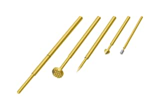
A contact probe is an inspection instrument used for continuity inspection by contacting the electrodes of various electronic components. Contact probes are widely used for inspection of electronic components. Various electronic components, such as semiconductors, liquid crystal panels, bare boards, PCBs, connectors, capacitors, sensors, and batteries, can be inspected using contact probes.
Contact probes are used not only in continuity checks but also to collect data for behaviour inspections of components in circuits (in-circuit tests) and for behaviour checks in function tests. In detail, contact probes are used to detect opens and short circuits, measure high frequencies, check impedance (resistance), and check parameters of components in circuits.
Structure of a contact probe
A contact probe consists of a barrel and, in the barrel, a spring and plunger that contacts inspection targets. The connection resistance in the barrel can be stabilised by optimising the spring pressure in the barrel. Typical contact probes contain parts plated with gold to prevent corrosion and decrease the contact pressure of sliding sections.
The required number of contact probes are pressed into a resin jig designed for the inspection target, and the plunger tips are brought into contact with this target. This instrument is highly maintainable because it can be used repeatedly simply by replacing the worn probes in the jig.
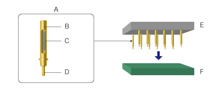
- A
- Contact probe
- B
- Barrel
- C
- Spring
- D
- Plunger
- E
- Jig
- F
- Inspection target
Plunger tip shapes of contact probes
The shape of the contact tip differs according to the shape of the inspection target such as electrodes and terminals. Using a plunger with the optimum tip shape prevents damage to fragile targets during inspection. Representative shapes and applications are introduced below.
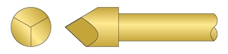
Round
This tip is used for inspection where damage to fragile electrodes, such as those on flexible printed circuits (FPCs), must be avoided.

Conical
This tip is mainly used to inspect lands and pads on PWBs.

Flat/Concave
A flat tip is used to prevent damage to electrodes or when the tip needs to contact an area on inspection targets.
A concave tip is used to contact the convex shapes of terminals.

Delta cone
A delta cone tip is used to inspect concave shapes such as through holes on PWBs.
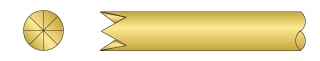
Crown
This shape is used to inspect the leads of mounting components and convex shapes by contacting with multiple probes.
Service Lives of Probe Cards and Contact Probes and Importance of Observation and Measurement
Service lives of probe cards
When a probe card is used to inspect LSI chips, multiple sharp and microscopic probe pins are brought into contact with chip terminals on wafers. Some small probe cards in the size of a few cm² have several thousand probe pins aligned at small pitches from 20 to 30 μm. Probe cards, which are very elaborate for contact inspection instruments, have service lives that are determined not by the number of years to be used but by the number of times probe pins contact chips on wafers. Typical probe cards are said to reach their service lives after performing hundreds of thousands to several million contacts.
When fabricating an enormous amount of chips using a large number of wafers, it is very important to understand the probe pin conditions to maintain product quality. Worn or abnormal probe pins can lead to the acquisition of incorrect inspection data, causing good chips to be rejected and decreasing the yield rate.
Service lives of contact probes
Electrical service lives of contact probes, each consisting of several parts and a tip with a microscopic and highly accurate shape, vary depending on the resistance, environment, and conditions allowed in inspection. Attention also needs to be paid to heat applied to the leads. Typical contact probes mechanically withstand approximately one million contacts.
This durability, however, varies depending on the inspection conditions. One item that is important in determining if a contact probe has reached its service life is to understand the shape of the plunger tip that contacts inspection targets. During inspection, worn tips can generate variations in resistance and cause false judgement, affecting the quality control and yield rate.
Importance of and problems in observation and measurement of probe cards and contact probes
Probe cards and contact probes both have contacts with microscopic shapes. To prevent inspection errors that can cause defective products to be overlooked or reduce the yield rate, periodic magnified observation and measurement are important in determining if instruments have reached their service lives due to wear or other reasons.
However, the inspection instruments have three-dimensional and microscopic contacts, which makes it difficult to observe the entire target clearly with optical microscopes because only a part of the target can be brought into focus under observation at high magnifications.
It is also difficult to accurately measure microscopic 3D shapes and dimensions, such as pin shapes and contact probe height, using contact measuring instruments because the probe of the measuring instrument, which is too large for the inspection target, simultaneously contacts multiple probe pins aligned at small pitches or applies measurement pressure. Dimension measurement is still difficult even when image processing is used because the entirety of these targets with microscopic shapes cannot be brought into focus.
Read on for an introduction to the latest examples of observation and measurement using our 4K digital microscope that solves these problems.
The Latest Examples of Wear Observation and Dimension and Shape Measurement of Probe Cards and Contact Probes
It is important to understand the microscopic shapes of probe card pins and contact probe plunger tips by observing and measuring damage such as wear because these shapes greatly affect the accuracy of electrical inspections. However, there are many problems in observation and measurement.
KEYENCE’s VHX Series 4K digital microscope is equipped with high-resolution HR lenses and a 4K CMOS image sensor, enabling it to accurately capture microscopic shapes of inspection instruments with high-resolution 4K images. This microscope can also perform 2D and 3D measurement accurately using observation images. Application examples of the VHX Series, which not only solves observation and measurement problems faced by inspection instruments but also improves the sophistication and efficiency of these operations, are introduced below.
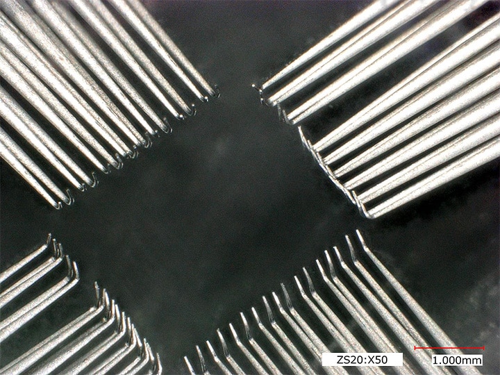
Observation of probe card pin contact and tilted observation
The VHX Series 4K digital microscope has both large depth of field and high resolution. High-resolution 4K images can be captured at any angle.
The free-angle observation system with high-accuracy XYZ motorised stage enables tilted observation at any angle with easy field-of-view alignment, rotation, and oblique axis motion.
High-resolution images can also be captured with handheld observation, allowing for observation even when the observation conditions are difficult to reproduce on the stage.

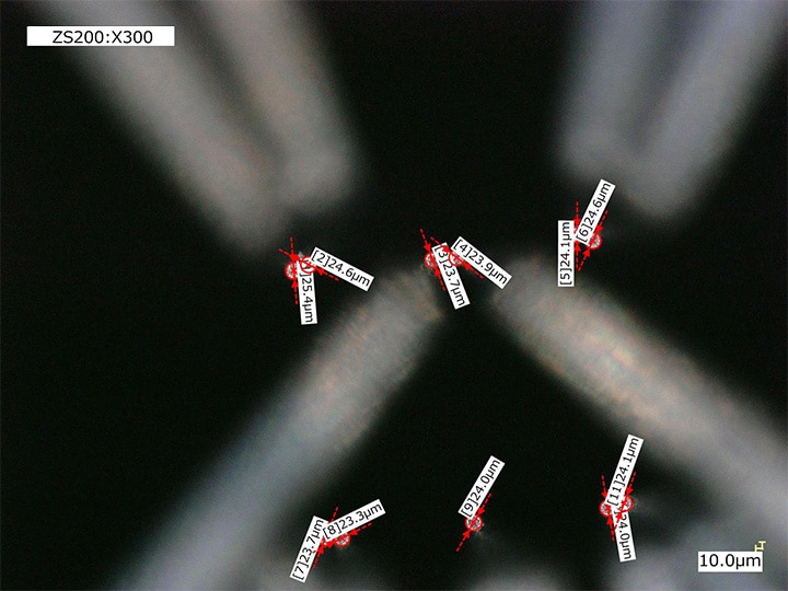
Outer diameter and height measurement of probe card pins
The VHX Series 4K digital microscope can perform highly accurate 2D and 3D measurement using clear observation images without touching the target.
Measured values of the outer diameter, required in order to understand wear on probe pin tips, can also be acquired in real time with simple mouse operations while watching the monitor. Various items, such as distances between two points, parallel lines, and areas, can also be measured in the same way.
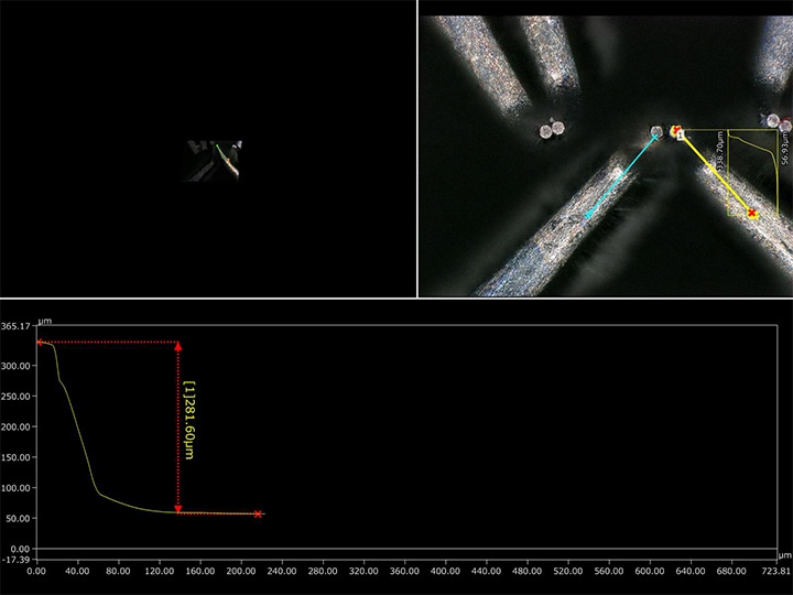
3D measurement can also be performed by acquiring pin height information. Profile measurement can also be performed by simply specifying a desired location, which enables easy acquisition of cross-section height values at the specified location.
High-magnification observation can be switched to non-contact dimension measurement seamlessly, improving the work efficiency. Measured values and images can be stored, and their history helps in understanding tendencies such as how wear and deformation progress.
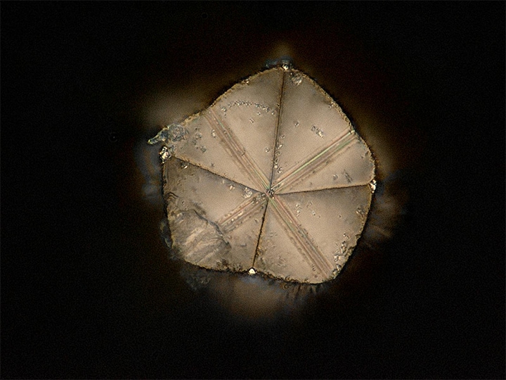
High-magnification observation of contact probe tips
The plunger tips of contact probes, which have microscopic three-dimensional shapes, wear out easily because they contact inspection targets. High-magnification observation of these targets often has a trade-off between requirements and conditions, resulting in, for example, images that are not focused throughout the entire field of view and reductions in resolution.
The VHX Series 4K digital microscope has both large depth of field and high resolution. This combination enables clear observation of microscopic wear and chipping of plunger tips using images that are focused throughout the entire field of view even at high magnifications.
Because the inspection instruments are made of metal, it takes a lot of time and effort to determine the lighting conditions due to the effects of diffused reflection. The VHX Series is equipped with the Multi-lighting function, which automatically acquires image data captured with omnidirectional lighting at the press of a button. Operators can promptly start observation simply by selecting the image suitable for the purpose, which significantly reduces the time required for lighting condition determination.
Additionally, the lighting conditions used when a past image was captured can be reproduced just by selecting that image. This increases the operation speed even when wear of multiple plunger tips needs to be observed under the same conditions.
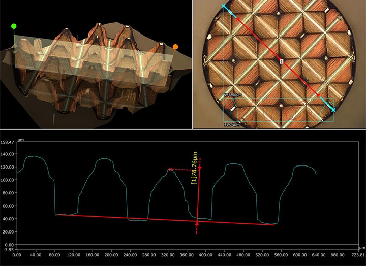
3D display and profile measurement of contact probe tips
The VHX Series 4K digital microscope captures multiple images at different focus positions and quickly composes them into an image to be used for highly accurate 3D display and 3D measurement. The 3D display even shows surface shapes and roughness, allowing for target observation at any angle.
Profile measurement can also be performed with the simple operation of specifying the desired location with the mouse. This enables acquisition of cross-section shapes and dimensions at desired locations in a non-destructive, non-contact manner.
With these functions, surface irregularities can be measured at sub-micrometre levels and the degree of wear can be understood with accurate values even when the plunger tip has a microscopic and complex shape.
A 4K Digital Microscope That Improves the Efficiency of Various Operations Including Accuracy Maintenance of Electrical Inspection
The high-performance and varied functions of the VHX Series 4K digital microscope strongly support not only the observation and measurement of inspection instruments having microscopic shapes but also the tasks of research, development, and quality assurance for various situations in the electronics field such as PWBs, cream solder application, and electronic device manufacturing and mounting.
A single VHX Series unit is all you need to observe with high-resolution 4K images, perform highly accurate 2D and 3D measurements, and even automatically create reports, greatly improving work efficiency. For additional product info or inquiries, click the buttons below.
